PCB-Forge
 CStudio.ao

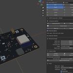
Installation and updates
Download PCB-Forge_2.5.0_Extension.zip without extracting it.
Open Blender and go to Edit > Preferences.
In Get Extensions, open the menu and choose Install from Disk.
Select the ZIP, complete installation and enable PCB-Forge.
In the 3D Viewport, press N and open the PCB-Forge tab.
When updating, save your project and disable the older installation first. Restart Blender after replacement. Enable only one installation format at a time.
Use the globe menu to choose the interface language. Save preferences to retain your choice.
Create your first board
Click Create board and choose a preset. Select the board object to display its parameters.
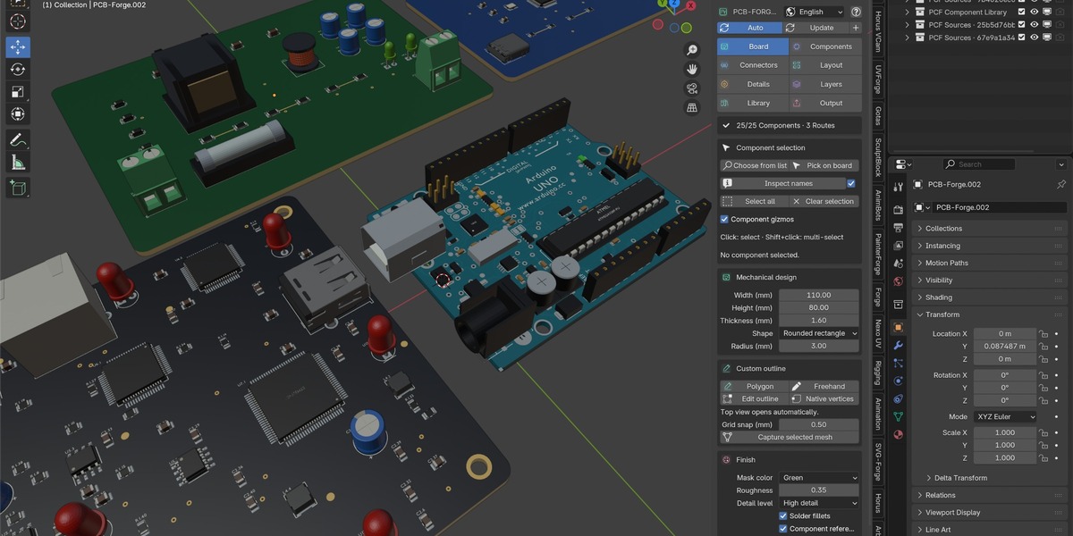
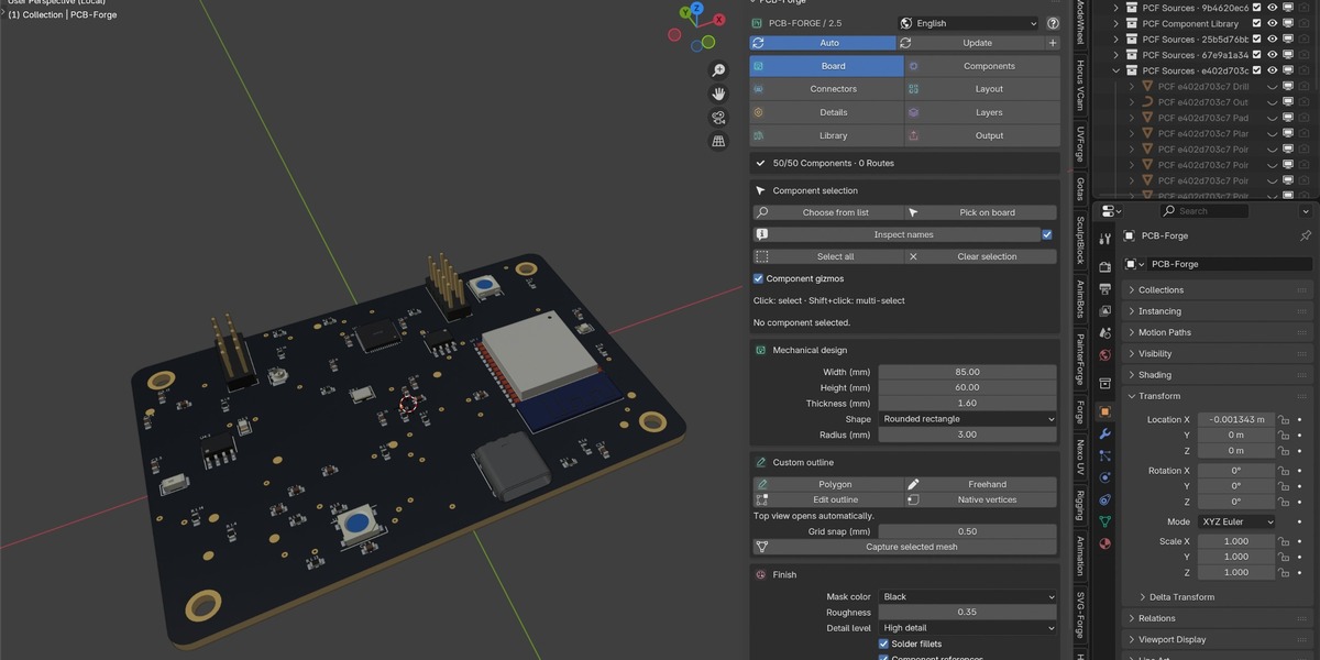
The main sections are Board, Components, Connectors, Layout, Details, Layers, Library and Output.
Presets are artistic compositions rather than verified working circuits.
If the board is isolated in Local View, use the numeric-keypad slash shortcut to leave Local View.
Dimensions and materials
In Board, adjust width, height, thickness, outline style, corner radius, mounting holes, solder-mask color and roughness.
Measurements are in millimetres. At Blender's default scale, 1 mm corresponds to 0.001 unit.
Change the add-on dimensions to recalculate the layout. Scaling the entire board object transforms the assembly without recalculating its mechanical dimensions.
Draw and edit an outline
Polygon: click each corner, then click the first point or press Enter to close. Shift aligns the next segment with an axis; Ctrl temporarily disables grid snapping.
Freehand: drag to sketch, release and apply. The sketch is simplified before use.
Edit outline: drag vertex markers. Shift-click an edge to insert a point, Delete removes a vertex and Backspace undoes a point operation.
Native vertices: edit the temporary filled mesh in Edit Mode. Select an exterior edge, press E, then Shift+Z, and move within the board plane. Confirm the transform and pause for the preview. Use Apply or Cancel in the PCB-Forge panel to finish.
Keep one closed, planar boundary without intersections or loose edges. Supported outlines contain 3–256 points, with dimensions of 8–1000 mm. Use the dedicated hole controls for internal openings.
The editor retains the last valid preview when the current boundary is invalid.
Optional area-based density can keep quantities, adapt passives/LEDs to area or adapt all groups. Apply commits the result; Cancel restores the initial outline, quantities and anchors.
Add and select components
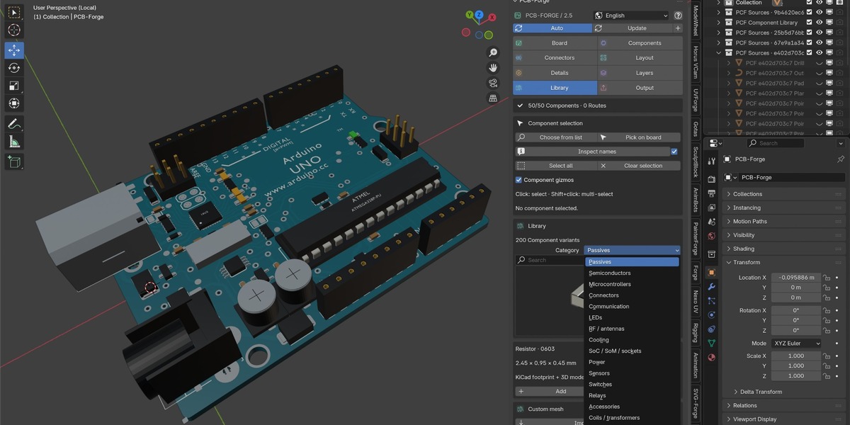
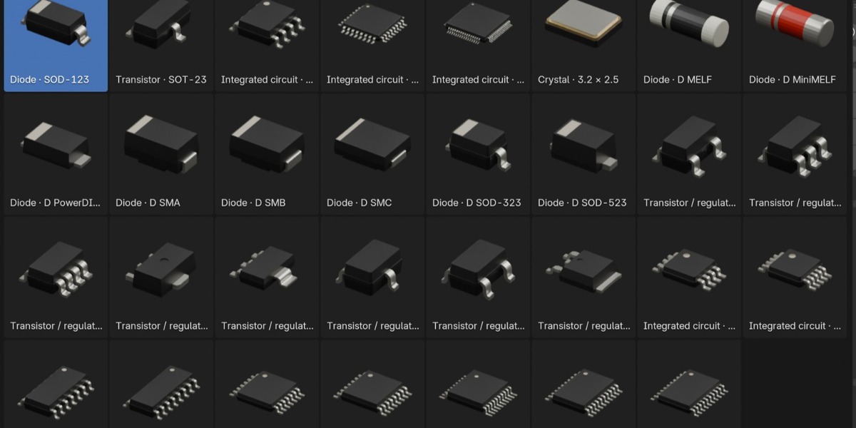
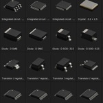
In Library, choose a category or search for a component, then select its thumbnail.
Add places a component automatically. Place with mouse starts interactive placement; Esc cancels it.
Component rows control quantity, variant, face, placement mode and enabled state. Limits are 500 components per row and 1500 requested components per board. Available space may reduce the placed quantity.
Click a component to select its instance, or use Choose from list. Shift-click adds or removes items from the selection. Check the editing face when selecting top-side or bottom-side components.
Hover names can be enabled independently of Inspector.
Move and rotate
Use viewport gizmos or Move selected to reposition the selection. Move component starts with a fresh pick.
Green preview bounds indicate a valid placement; red indicates a conflict. Confirm to apply or press Esc to cancel. Free neighbours can relocate around edited components.
Rotate using the dial, angle-step buttons or numeric Position / rotation controls. During interactive movement, R rotates by the configured step and Shift+R reverses it.
Scale individual components
With components selected and the pointer over the viewport:
• S: adjust scale interactively.
• S, 2, Enter: multiply the current scale by two.
• S, 0.5, Enter: reduce the current scale by half.
• S, X/Y/Z, value, Enter: constrain scaling to a local component axis.
• Press the same axis again to return to uniform scaling.
• Enter or left-click: confirm.
• Esc or right-click: cancel.
• Backspace: edit a typed number.
• Shift: finer pointer adjustment.
• Ctrl: adjustment in 0.1 steps.
Scale XYZ provides absolute factors relative to the original model. Reset scale returns those factors to 1. The S tool applies a multiplier to the current size.
Positive factors range from 0.05 to 20 per axis. Global component scale and fit settings still apply. Placement constraints can reject a change that cannot preserve the placed quantity.
Body geometry, terminals, pads, holes and silkscreen follow the transformation. Recalculate copper routes after changing pad geometry.
Duplicate, align and delete
Multi-selection supports group transforms, duplication with an offset, alignment and distribution. Invalid group transforms are rejected together.
Delete this instance removes only the selected part, its anchor, scale data and associated connections. Remove group deletes the entire quantity row.
These editing operations support Blender undo/redo.
Layout and anchors
Adapt scale can shrink the overall component mix to fit. Keep real dimensions reports placement shortages instead.
Clearance, edge margin, seed and Keep neighbour positions influence placement.
Manual edits anchor the affected instances. Release pin or Release all pins restores automatic positioning while retaining individual scale.
Heat sinks and sockets have mounting-height controls that participate in collision checks.
Preview and detail level
Fast preview uses simplified geometry and omits solder fillets and reference text. High detail adds those details where space allows.
Generated geometry remains instanced until realization or export.
Connections and routing
In Details, enable traces and use Connect pads to select actual source and destination terminals. Assign a net name. Connections sharing the same named net may branch.
Use the pencil control to rename a net across its connections.
Click Route connections to calculate paths. The default routing uses horizontal, vertical and 45-degree directions. Width, clearance and corner cut control their appearance.
Paths are checked geometrically against board borders, holes, pad bounds, components and copper from other nets.
Dashed connections are unresolved or need recalculation. Route again after moving components or changing the outline. Dense layouts can remain unresolved because routing uses a bounded search budget.
Vias, pads and copper planes
Opposite-face connections can use one routed via when enabled. Both external-face route segments must succeed. This is not arbitrary internal-layer routing.
Copper planes use a selected net, face and grid resolution. They maintain conservative clearance and remove unconnected floating regions.
Decorative vias, test pads, manual pads and drilled holes have separate controls.
These tools provide visual geometry. They do not implement fabrication DRC or thermal reliefs.
Layer presentation
In Layers, choose 2–16 represented copper layers. Increase the layer gap for an exploded view and return it to zero for an assembled presentation.
This is a visual stack rather than a validated electrical stackup.
Import a custom mesh
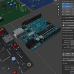
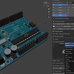
Select the source mesh, then select the PCB last so it is active. Use Library > Custom mesh > Import selected mesh.
The evaluated geometry, materials and relative transform are captured as an internal source. The original mesh remains in the scene.
Importing does not generate electrical pads or a footprint automatically. It is not a STEP-import workflow.
Save and export
Save the original .blend to retain parameters, outlines, instance IDs, anchors, scales and connections. Keep the helper PCF collections because the generated node graph references them.
Output provides Duplicate board, Create mesh copy, Organized assembly, Export GLB / OBJ and Save to Asset Browser.
Organized assemblies contain a root, board/details and separate component objects.
Exports also include a .pcb-forge.json metadata file. This is not a manufacturing netlist.
Asset Browser export writes a .blend collection asset. Refresh the Asset Browser and save preferences when registering its folder.
Exported assets are mesh assemblies. Keep the original parametric project for future parameter changes.
Manual edits to the generated node graph may be overwritten when the add-on rebuilds it.
Compatibility and support
Target: Blender 4.5+. Developer-tested on Linux with 4.5.3 LTS and 5.0.1. Native Windows/macOS validation is pending.
For support, contact the creator through Superhive. Include the add-on version, Blender version, operating system and reproduction steps. Add a screenshot or small reproducible project when helpful.
Code and bundled asset licenses are included in the package. See THIRD_PARTY_NOTICES.md for third-party credits and conditions.
Have questions about this product?
Login to message
| Published | about 2 hours ago |
| Blender Version | 4.5 - 5.2 |
| Extension Type | N/A |
| Render Engine Used | Blender-Internal, Cycles, Eevee |
| License | GPL |

Discover more products like this
circuit-board hard surface parametric pcb geometry nodes modeling procedural components sci fi Electronics